Design & specifications#
If you want to know how BeagleV Ahead board is designed and what are it’s high-level specifications then this chapter is for you. We are going to discuss each hardware design element in detail and provide high-level device specifications in a short and crisp form as well.
Block diagram#
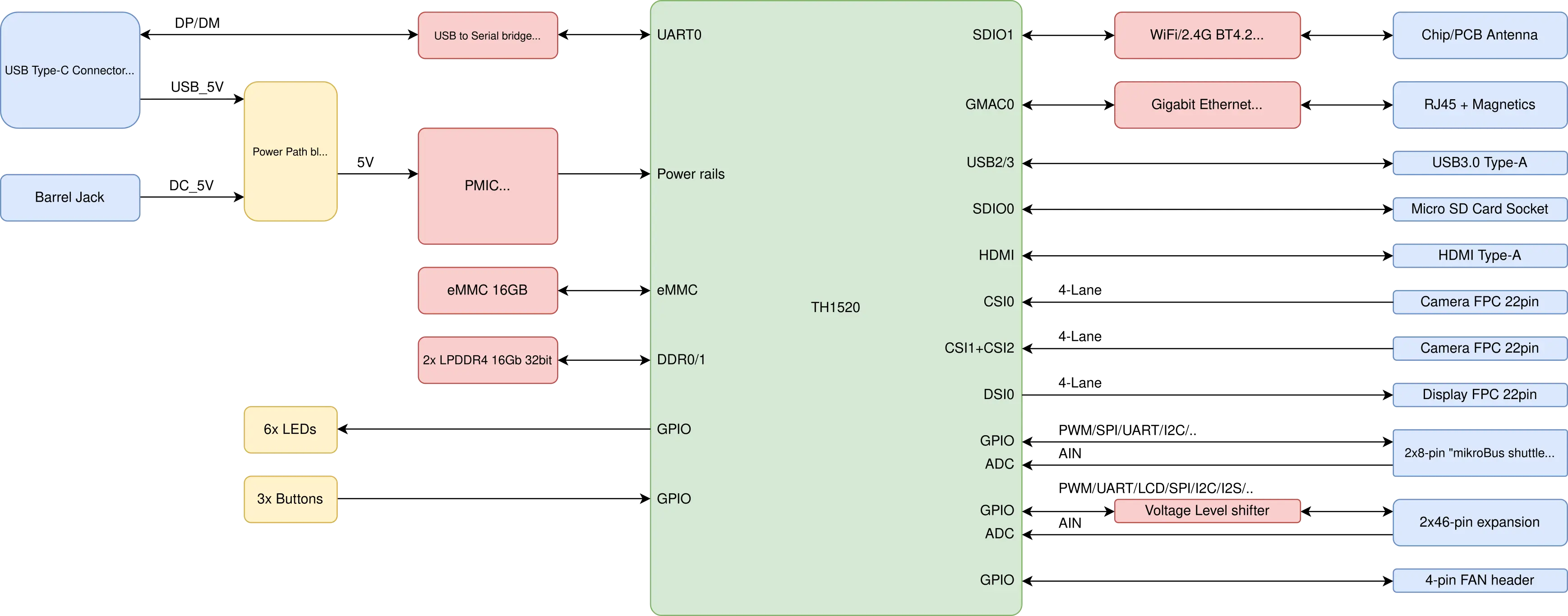
Fig. 386 System block diagram#
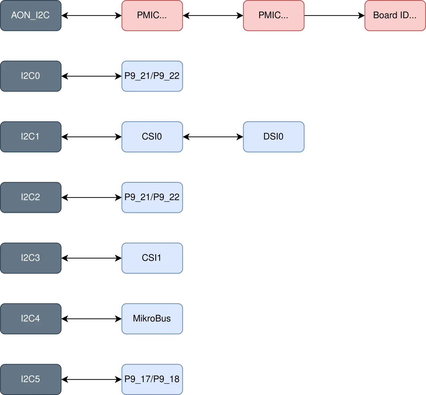
Fig. 387 I2C-Usage diagram#
System on Chip (SoC)#
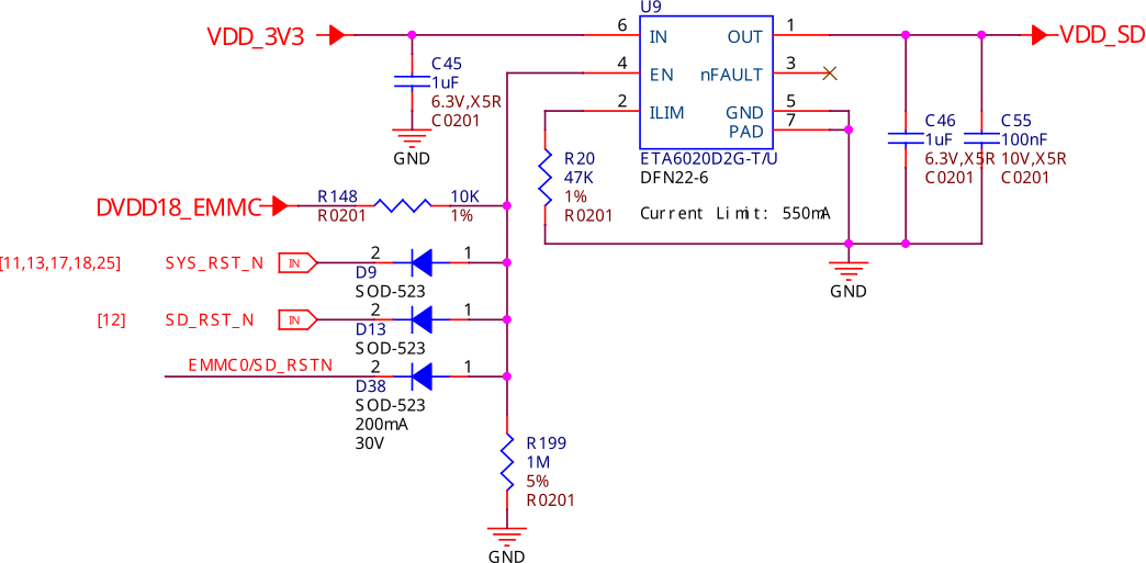
Fig. 388 SoC eMMC power switch#
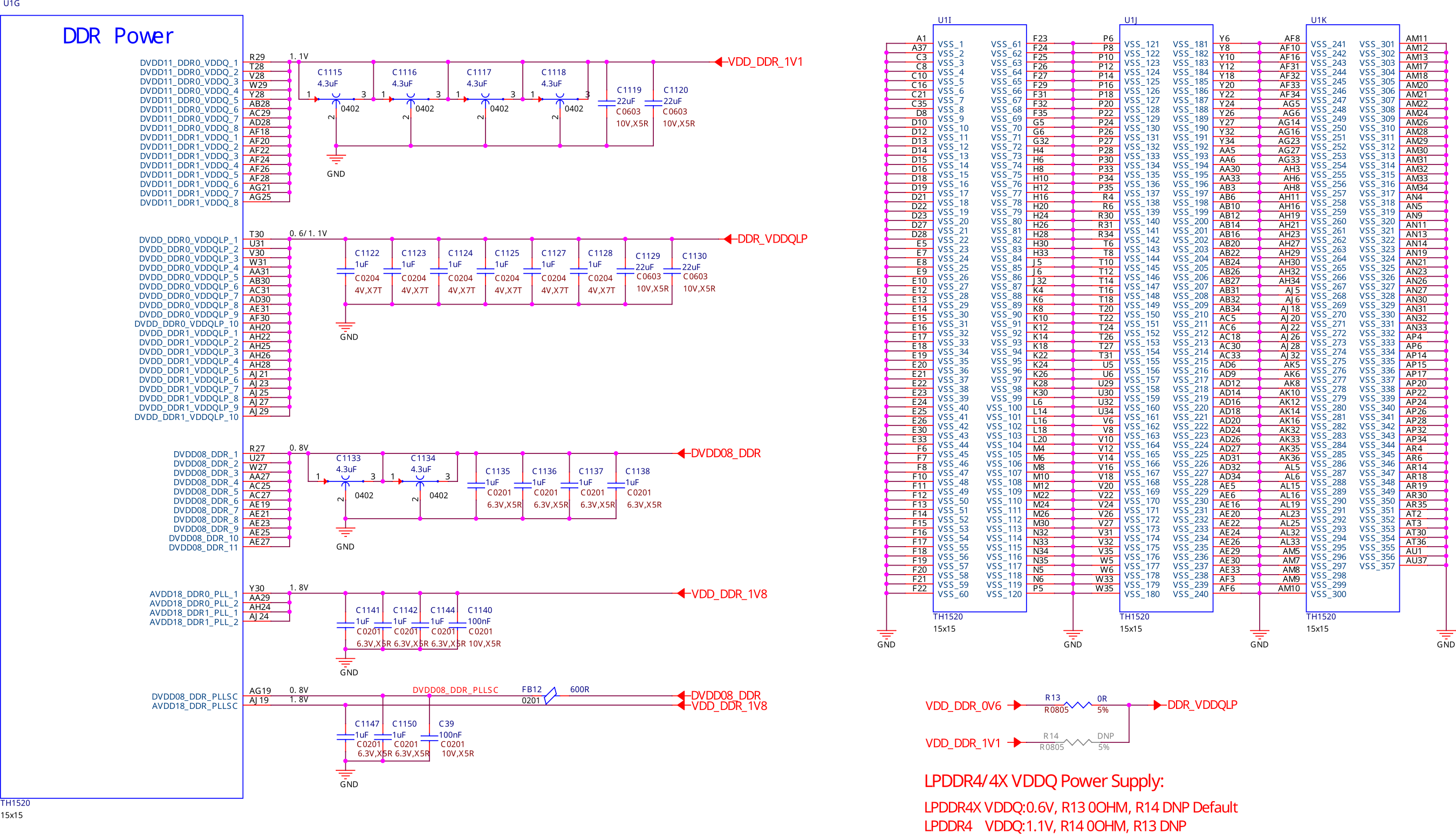
Fig. 389 SoC DDR Power#
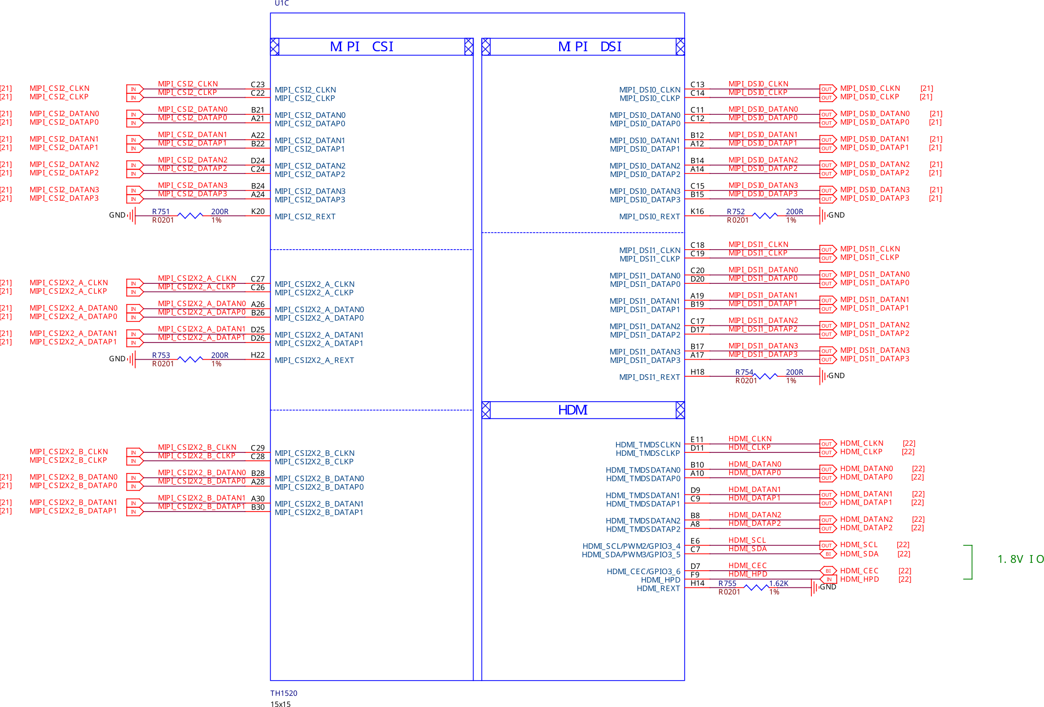
Fig. 390 SoC MIPI CSI DSI HDMI#
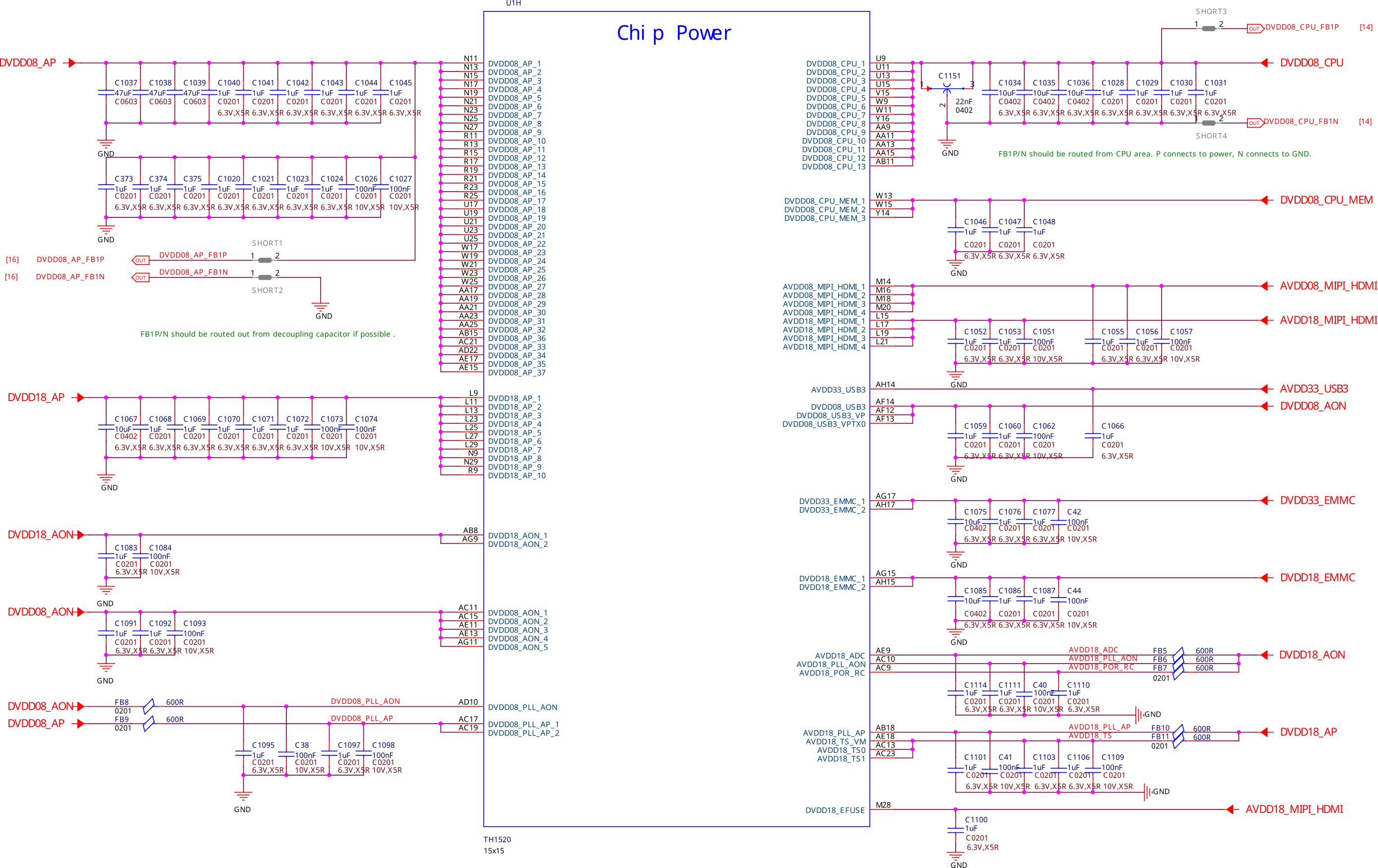
Fig. 391 SoC power#
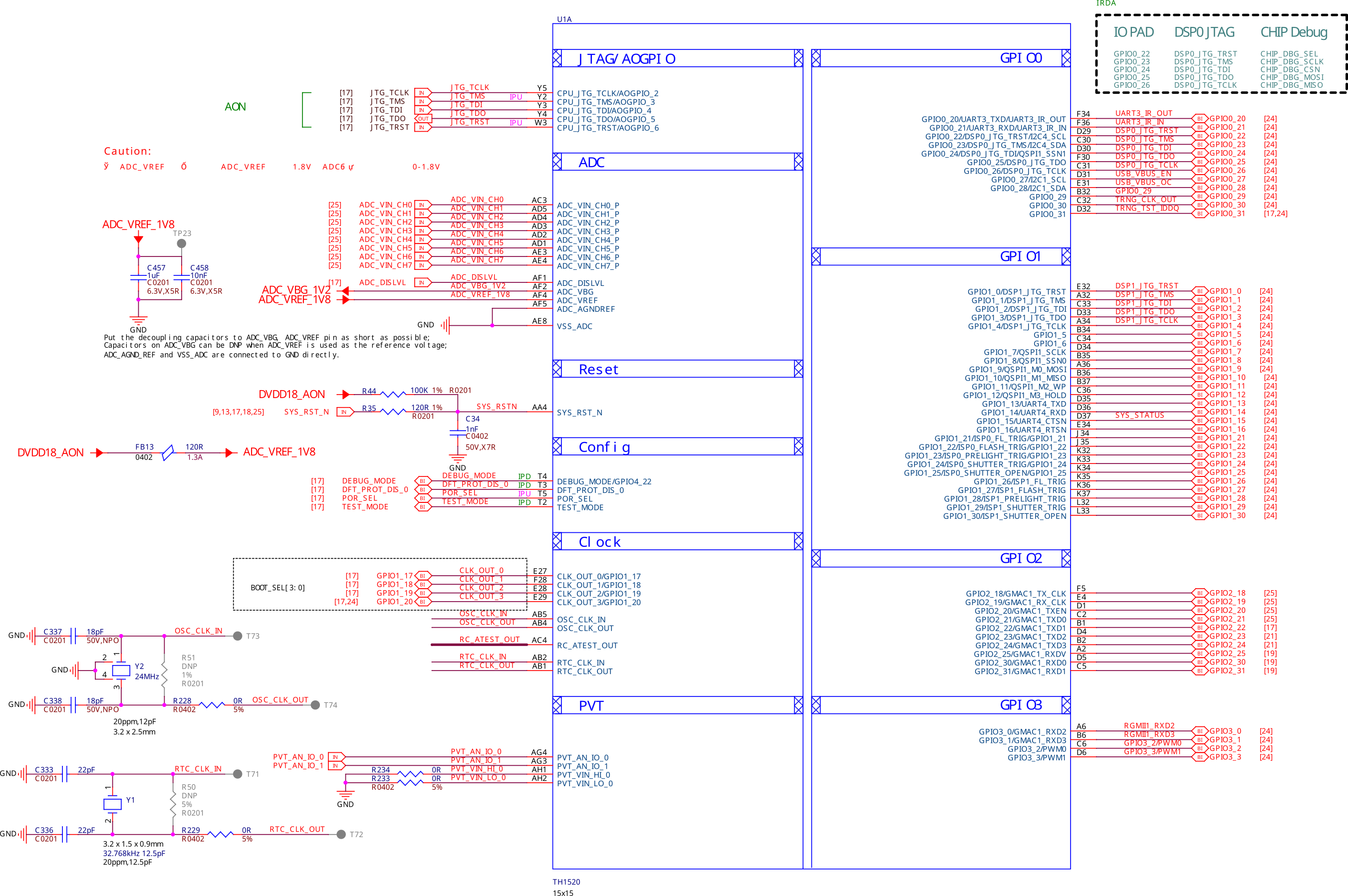
Fig. 392 SoC sys, ADC, and Clock#
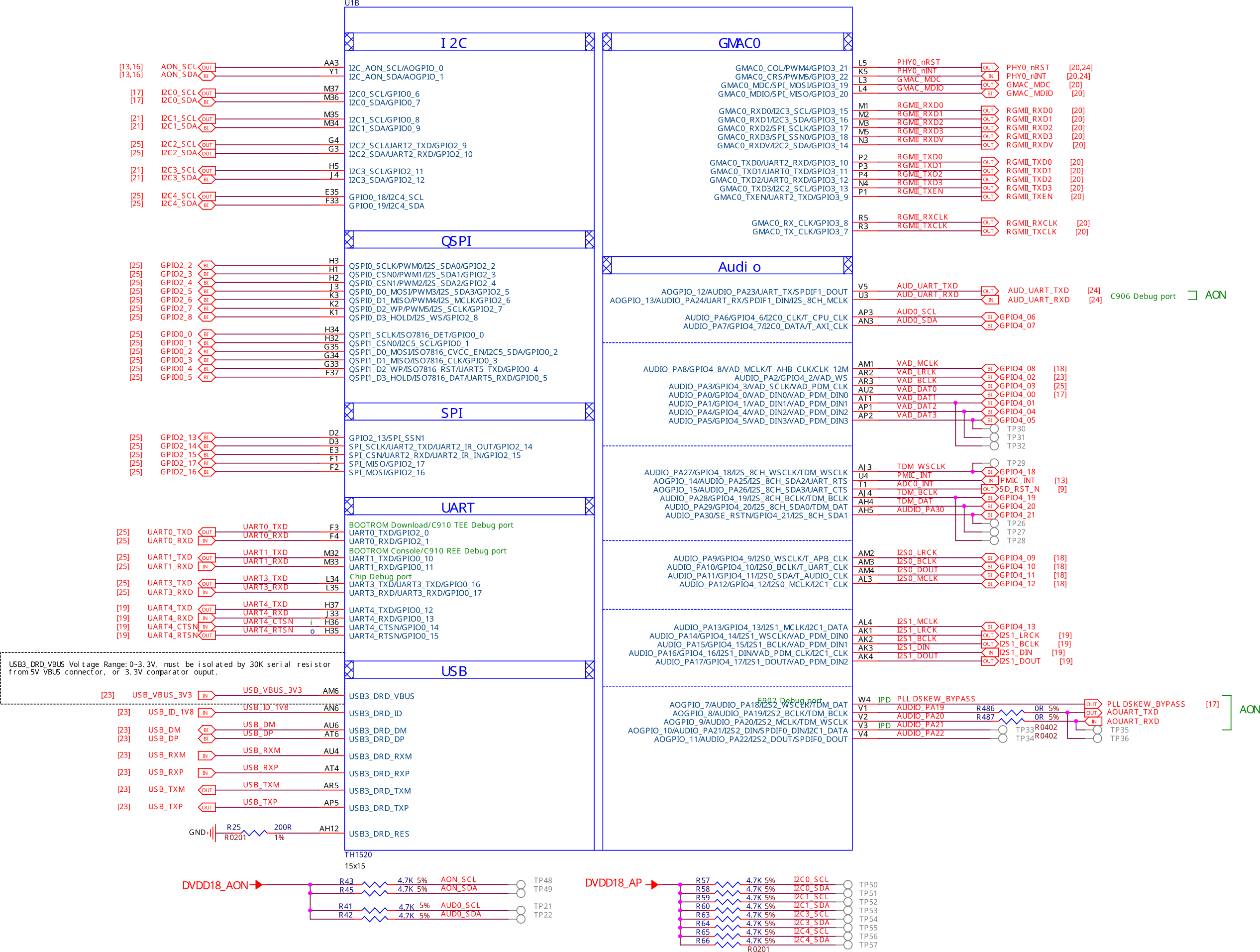
Fig. 393 SoC USB GMAC Audio#
Power management#
Barrel jack#
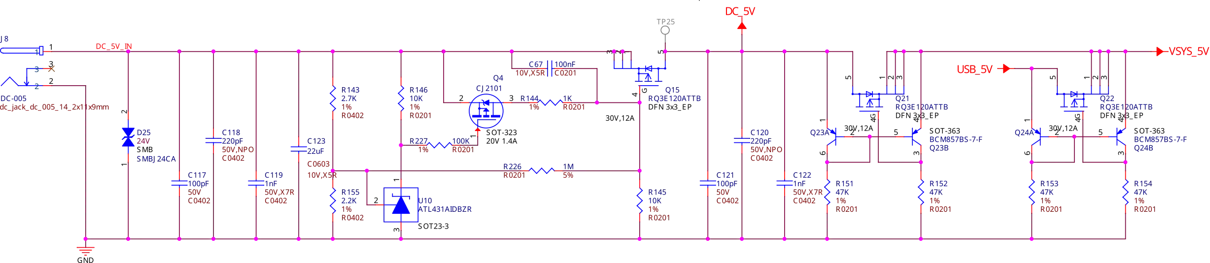
Fig. 394 Barrel jack power input#
0.8V DCDC buck#
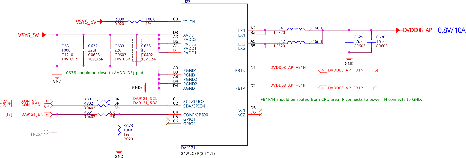
Fig. 395 0.8V DCDC buck converter#
3.3V DCDC buck#
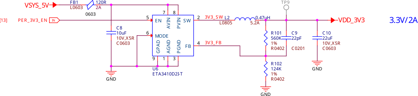
Fig. 396 3.3V DCDC buck converter#
1.8V LDO#
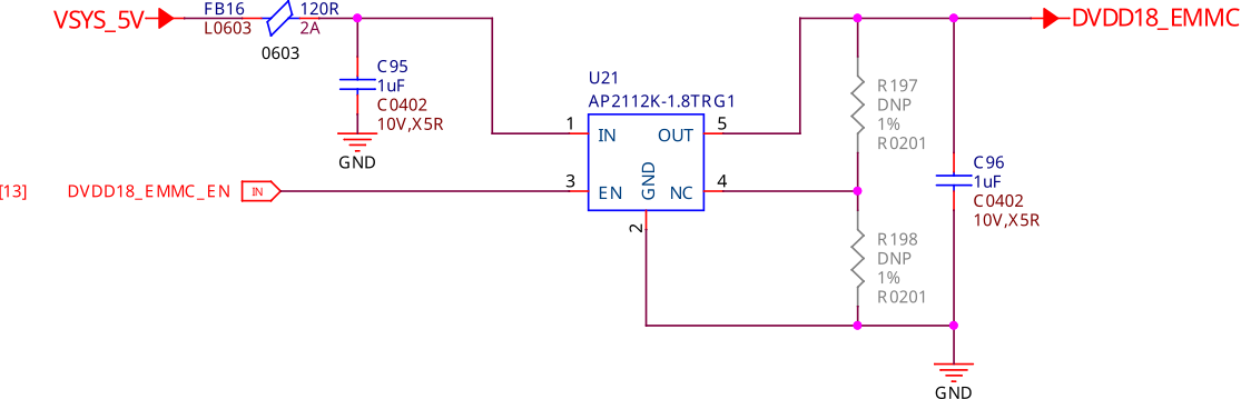
Fig. 397 1.8V LDO regulator#
PMIC#
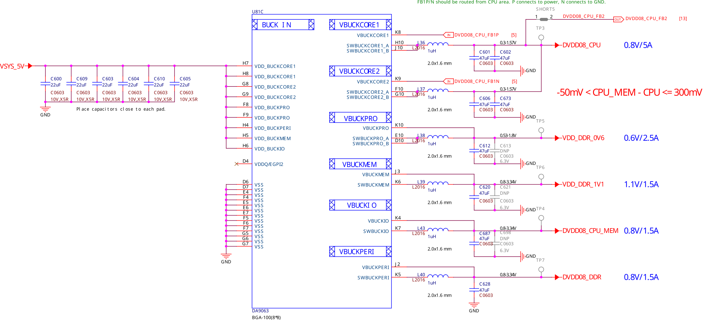
Fig. 398 PMIC Buck#
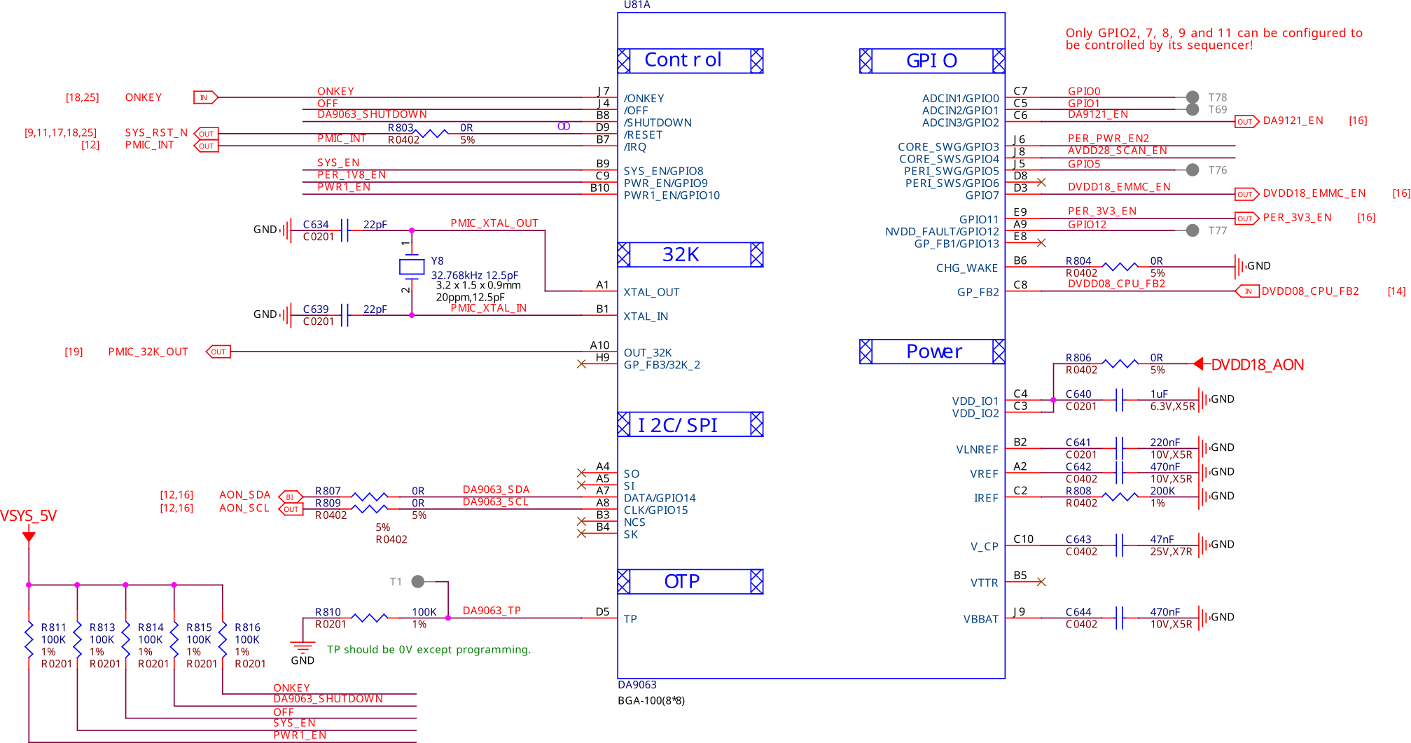
Fig. 399 PMIC Control#
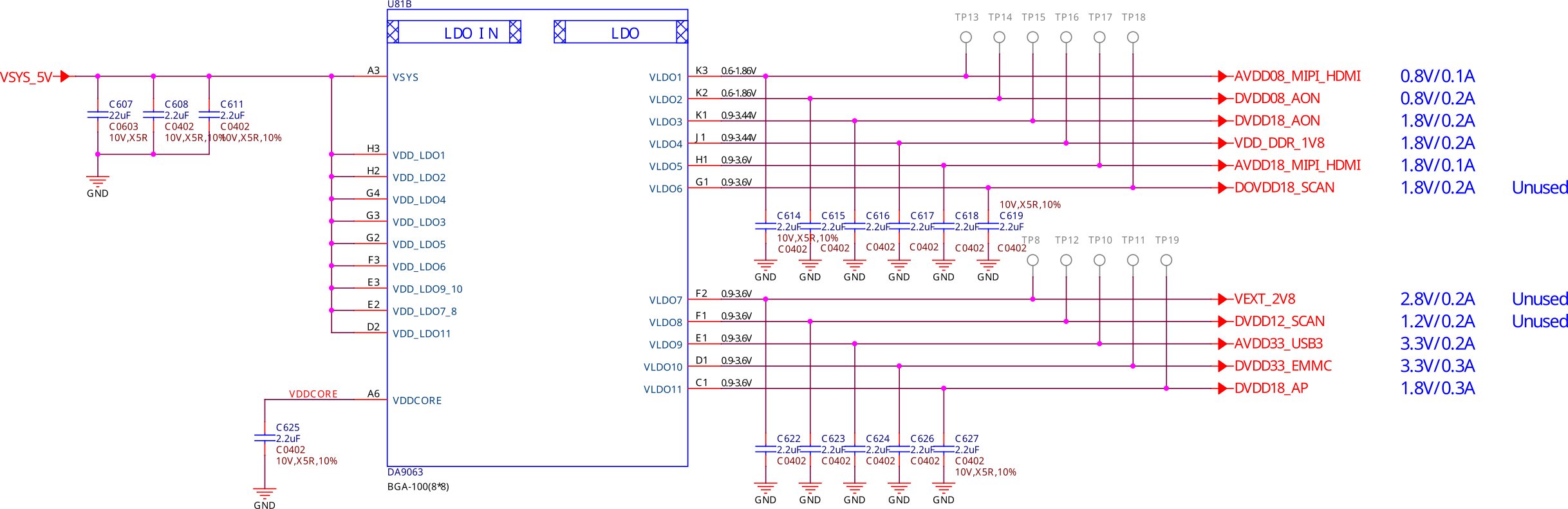
Fig. 400 PMIC LDO#
General Connectivity and Expansion#
microUSB 3.0 port#
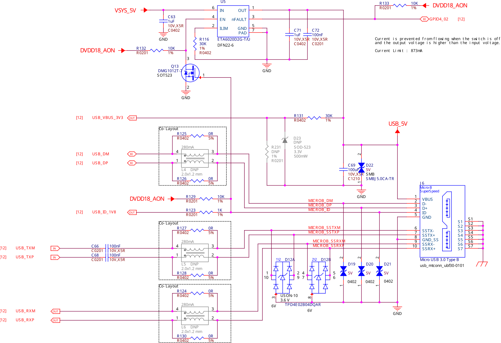
Fig. 401 microUSB 3.0 port#
P8 & P9 cape header pins#
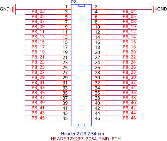
Fig. 402 P8 cape header#
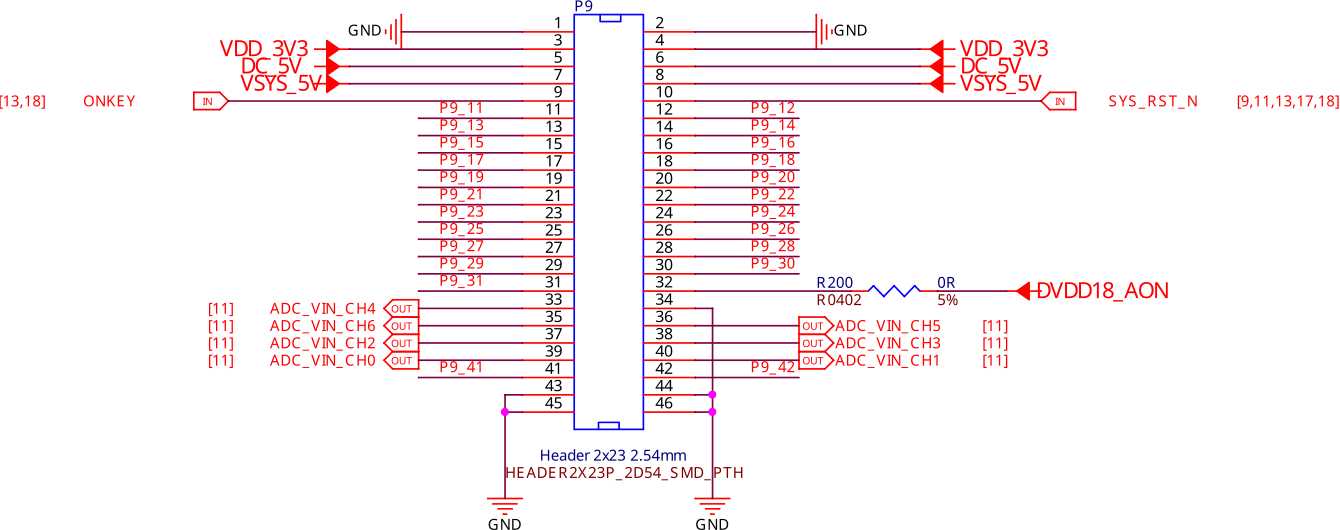
Fig. 403 P9 cape header#
mikroBUS shuttle connector#
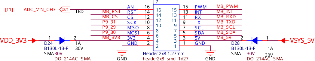
P8, P9, and mikroBUS helper circuitry#
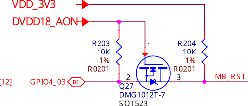
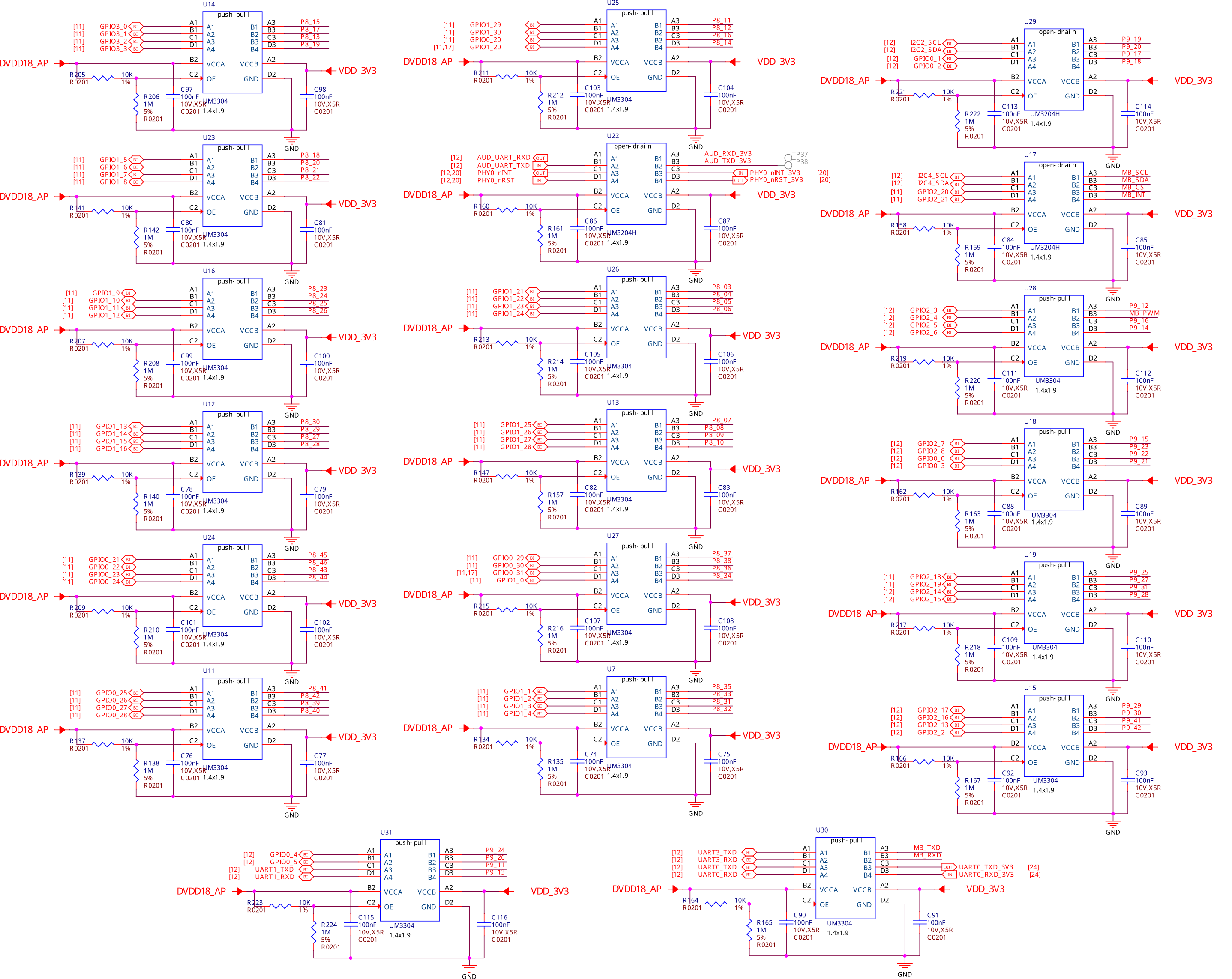
Fig. 404 P8, P9, and mikroBUS level shifters#
Buttons and LEDs#
Boot select buttons#
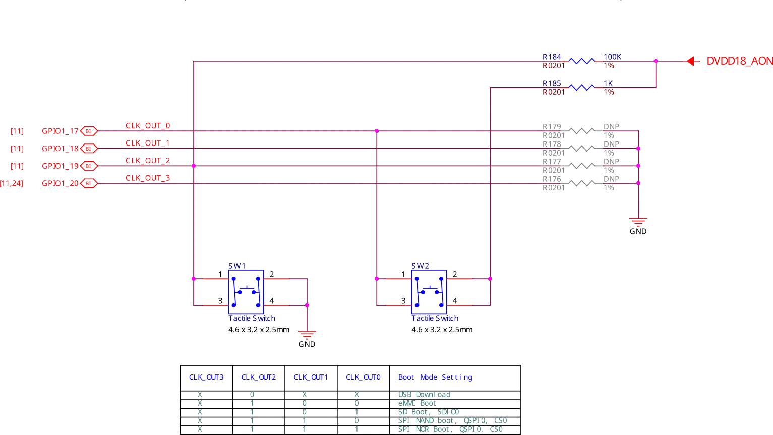
Fig. 405 Boot select buttons#
User LEDs and Power LED#
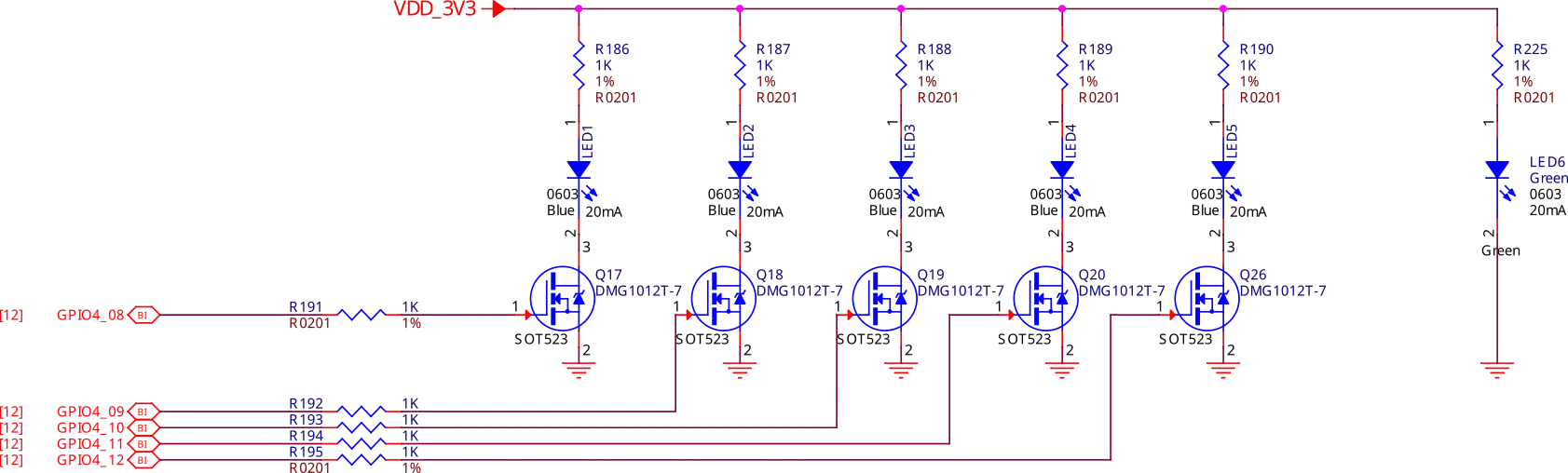
Fig. 406 User LEDs and power LED#
Power and reset button#
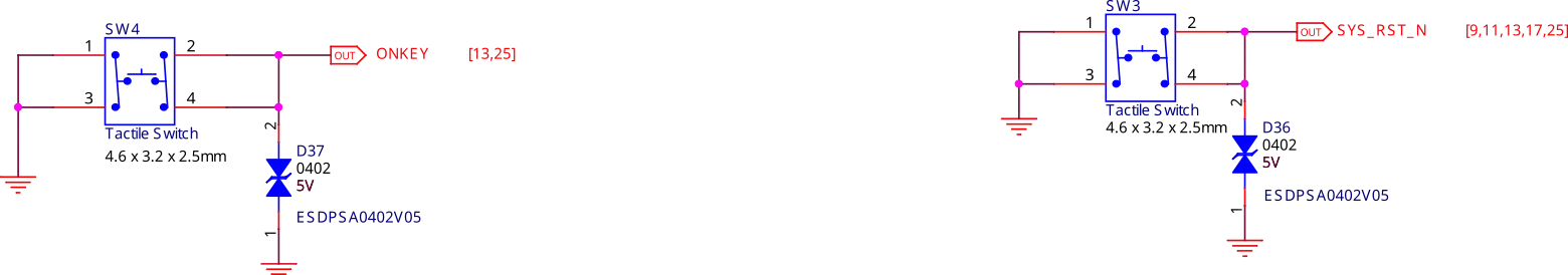
Fig. 407 Power and reset button#
Wired and wireless connectivity#
Ethernet#
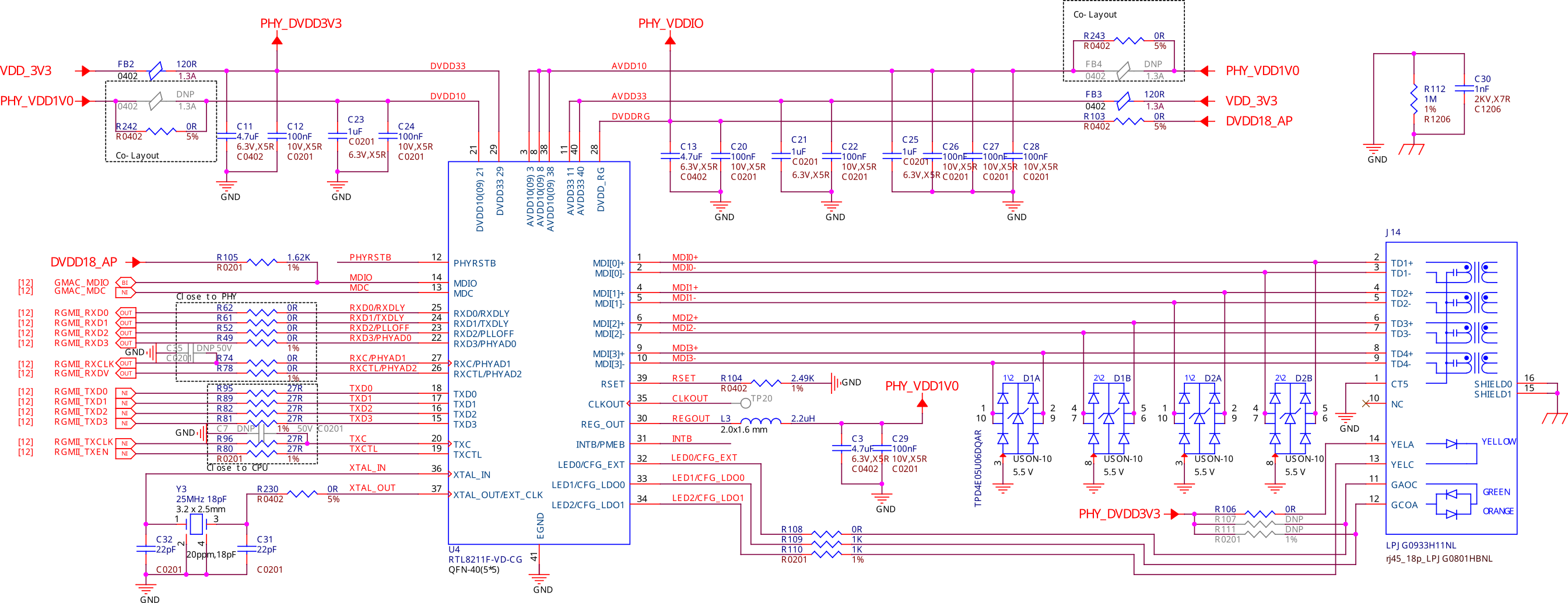
Fig. 408 Ethernet#
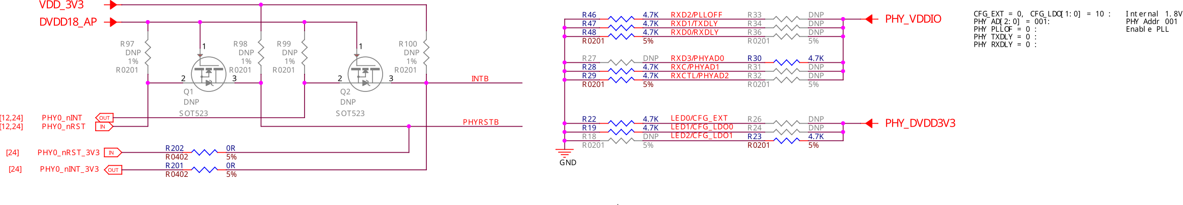
Fig. 409 Ethernet LevelShifter and Strapping#
WiFi & Bluetooth#
Fig. 410 WiFi and Bluetooth#
Memory, Media and Data storage#
DDR memory#
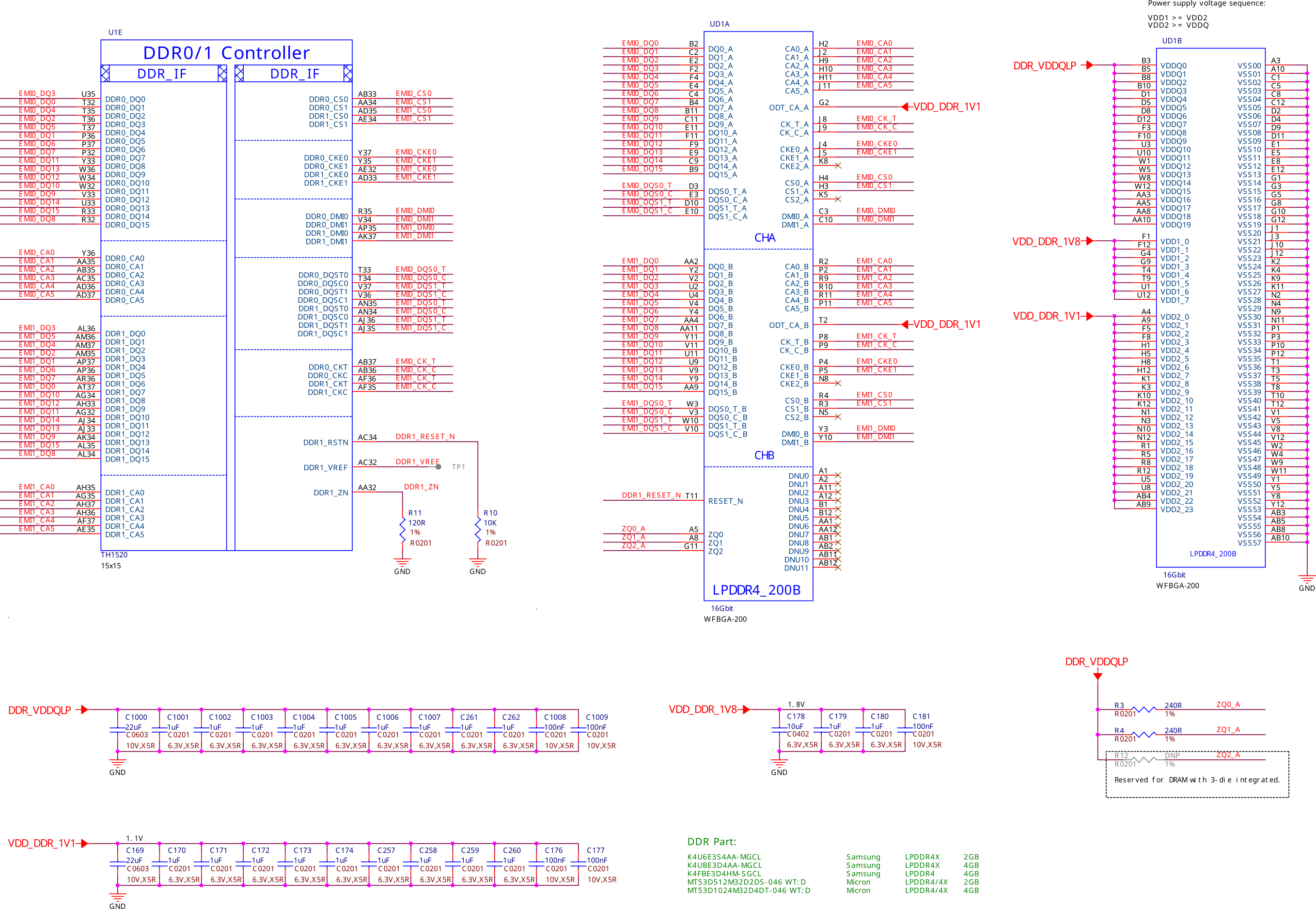
Fig. 411 2GB DDR4 Memory chip1#
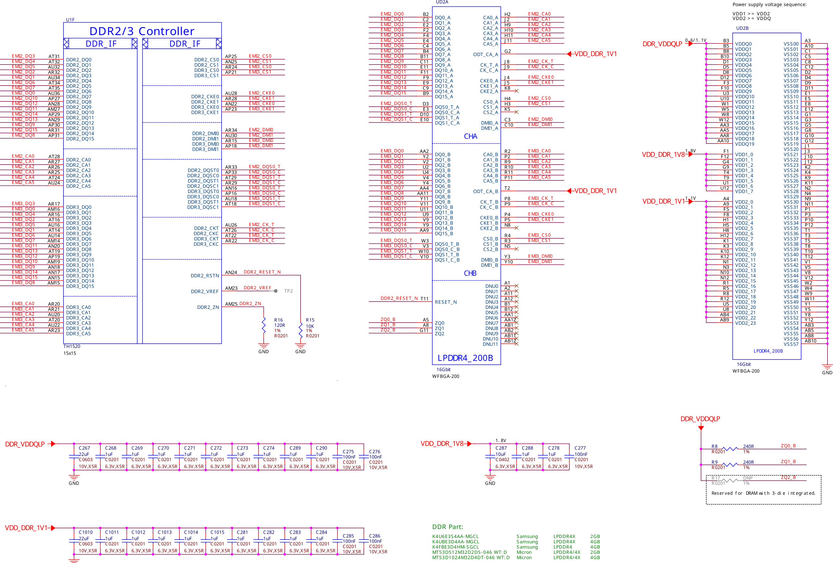
Fig. 412 2GB DDR4 Memory chip2#
eMMC#
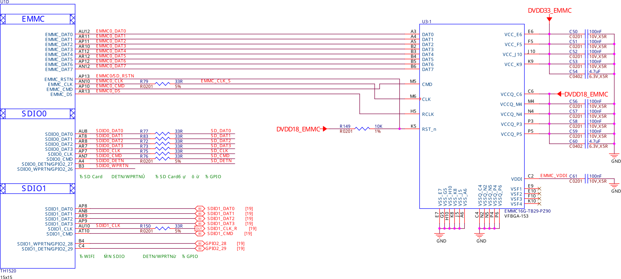
Fig. 413 16GB eMMC#
microSD#
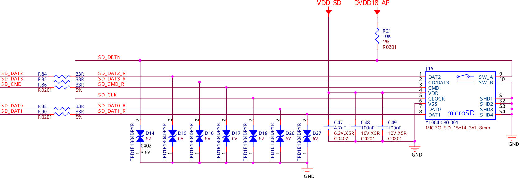
Fig. 414 microSD card connector#
EEPROM#
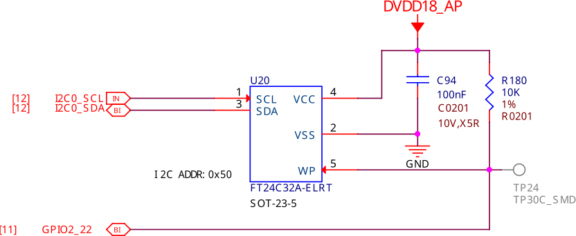
Fig. 415 16GB EEPROM#
Multimedia I/O#
CSI0#
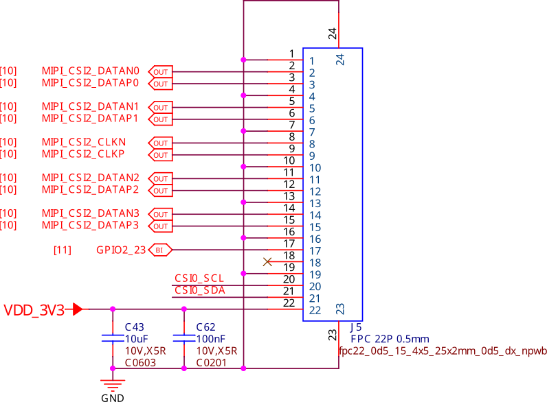
Fig. 416 CSI0 camera interface#
CSI1#
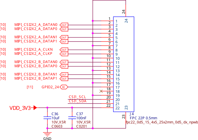
Fig. 417 CSI1 camera interface#
DSI#
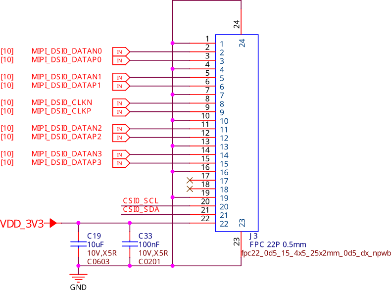
Fig. 418 DSI display interface#
CSI & DSI level shifter#
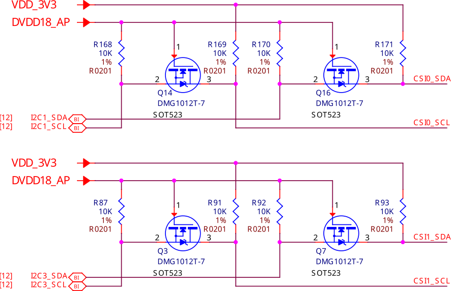
Fig. 419 CSI & DSI level shifter#
HDMI#
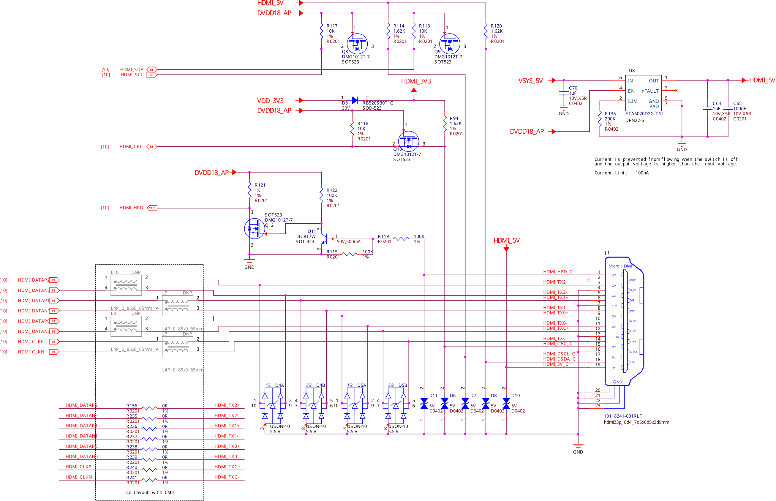
Fig. 420 HDMI display interface#
Debug#
UART debug port#
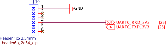
Fig. 421 UART Debug port#
JTAG debug port#
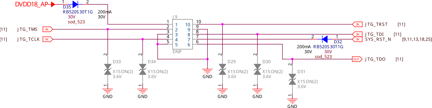
Fig. 422 JTAG debug port#
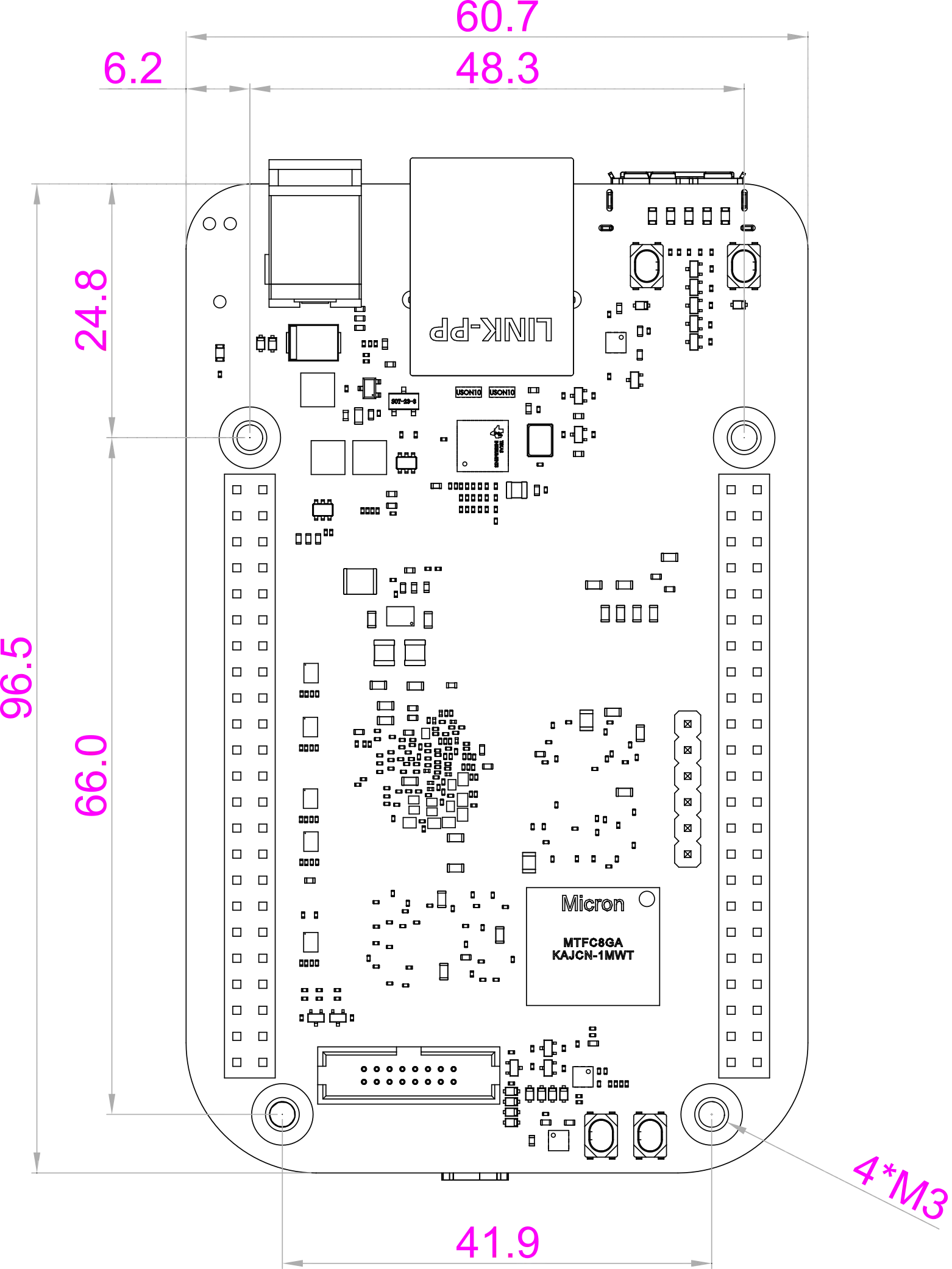
Mechanical Specifications#
Top |
Bottom |
|---|---|
|
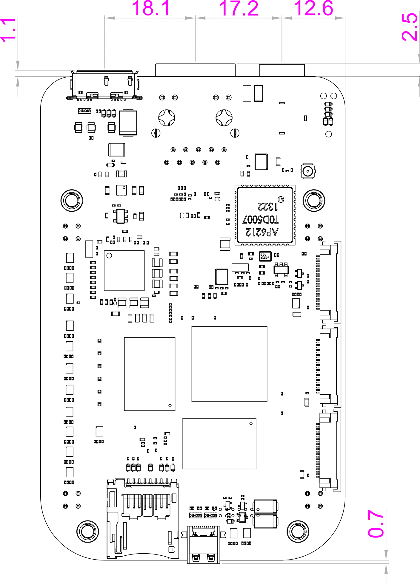
|
Front |
Left |
Right |
|---|---|---|
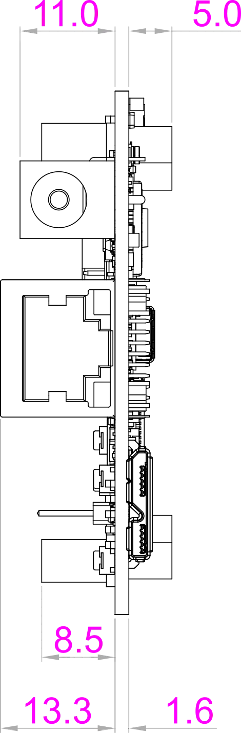
|
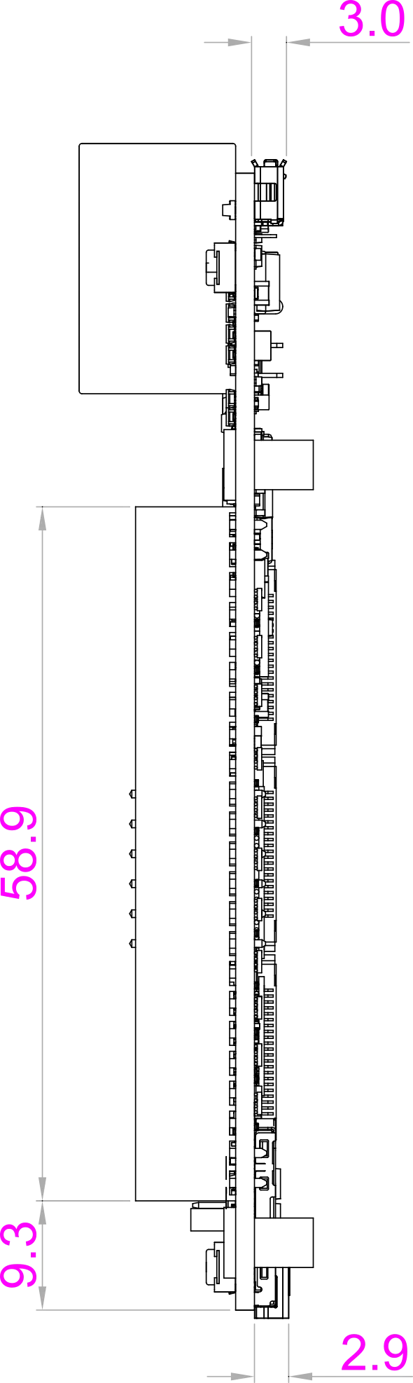
|
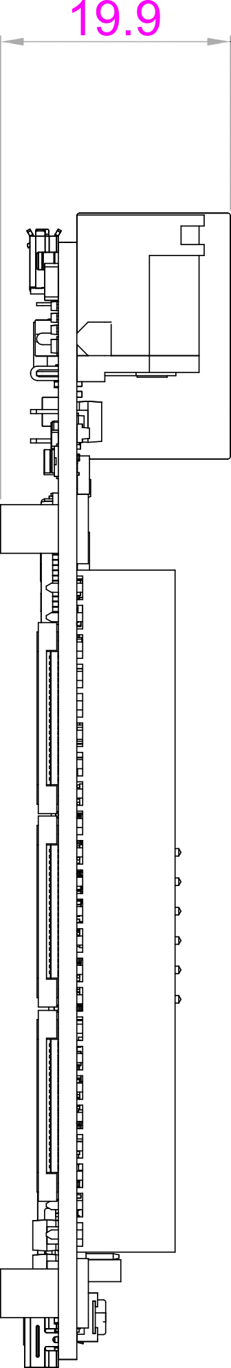
|
Parameter |
Values |
|---|---|
Size |
96.5×60.7×19.9mm |
Max heigh |
21.1mm |
PCB Size |
96.5x60.5*1.6mm |
PCB Layers |
10 layers |
PCB Thickness |
1.6mm |
RoHS compliant |
yes |
Gross Weight |
128.8g |
Net weight |
49.7g |
